


 Serviços customizados
 Inglês (pdf)
 Artigo em XML
 Referências do artigo
 Enviar este artigo por email
 Citado por SciELO
  Similares em
SciELO
Similares em
SciELO 
 Permalink
1.-INTRODUCTION
Researchers have studied the antennas since they are main part of wireless communication systems [1,2]. With the increasing demand of higher data rate, better coverage, capacity, reducing power consumption, interference suppression and multipath mitigation; more efficient radiation systems are needed. Smart antennas give a promising future in order to achieve the goals above mentioned by introducing a space division multiple access (SDMA) in new generations of wireless networks. This medium access technique provides spatial filtering to face high level of interference environments.
There are three kinds of smart antennas: switching beam antennas, phased arrays and adaptive smart antennas (ASA). The former can focus the radiation pattern to a finite number of angles, switching between lobes in order to maximize the signal-to-noise power ratio (SNR). The second can adjust dynamically the feeding progressive phase of the array cells for steering the main lobe, covering a continuous range of angles [3]. The last combines array antenna and digital signal processing theory to make a smarter system.
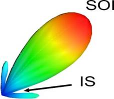
ASA, by means of an adaptive algorithm, modifies the amplitude and phase of the signal at each unit cell of the array for steering the main lobe to signal of interest (SOI) and nulls to interference signals (IS) [4], as shown in Figure 1.
Different Adaptive algorithms have been used for digital beamforming such as least mean square (LMS), normalized least mean square (NLMS) and recursive least square (RLS) [5]. These algorithms are no blind because they need prior information of the SOI, which is normally used as reference or training signal. Some blind algorithms such as constant modulus algorithm, have been proposed mainly in systems where info about SOI is hard to be obtained [6].
Authors have used LMS adaptive algorithm in smart antenna analysis and designs [5,7-11] by its robustness, simplicity and low computational cost. Comparative studies between LMS and others adaptive algorithms have been reported on literature [5,7,10,11].
In [5] LMS and NLMS were compared based on normalized array factor and mean square error (MSE) for mobile communications. They have high resolution for beam formation, but LMS has better performance minimizing the MSE. LMS, RLS and SMI were studied in [7] founding the former has minor side lobe level and major main beam level to side beam level ratio. However, its slow convergence presents problems tracking signals in high velocity environments [11].
Radio Frequency Identification (RFID) technology uses radio frequency signals to identify tagged objects. It consists of RFID readers and tags, which are attached to single objects. The data code contained in the tag allows the identification of the object. Improvement RFID systems are the subject of much research [12-33].
Capabilities of these systems as automatic identification, real time location tracking and sensing the surrounding result in an increase of RFID application areas: health care, traffic, airports, banks, schools, access control, security, libraries and smart inventory [13,16,25].
However, RFID applications demand to eliminate limitations as cost, interferences, collisions and energy efficiency [13,16,33]. Anti-collisions algorithms based on time division multiple access (TDMA) have been studied in recent years. In order to improve energy efficiency a power optimization waveform was proposed in [30] and authors have designed array antennas [15,19,20,22,23,26,32]. Smart antennas have been used for more efficiency power allocation, reducing the level of interference and achieving more coverage area for readers [19,20,32].
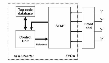
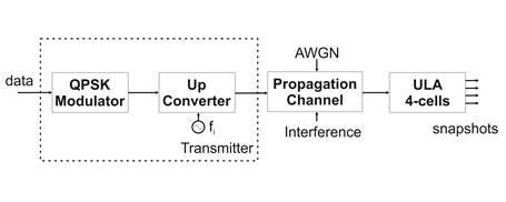
This work is in the context of enhancing the interrogation range, radiation performance, interferences mitigation and reduce the number of RFID readers. For accomplishing this goal a space time adaptive processing (STAP) is used. Unlike the designs reported in the literature, a non-blind LMS algorithm is implemented to achieve a low computational cost design. A general diagram of this kind of readers is shown in Figure 2. The use of IQ beamformer and digital down converters (DDCs) allow replacing the traditional super-heterodyne receiver by low-IF sampling down conversion.
This paper is organized as: In section 2, the mathematical model for the proposed system is described. Section 3 presents a simple channel implementation and analysis of LMS algorithm. Section 4 exhibits the proposed STAP design. Section 5 shows the system performance. In section 6, a resume of resource consumption on FPGA z7020 is presented. Section 7 concludes this paper.
2.-MATHEMATICAL ADAPTIVE SMART ANTENNA MODELING
Figure 3 shows a block diagram of an ASA system with STAP, which is composed by a uniform lineal array (ULA), front-ends for each antenna array cell, analog-to-digital converts (A/D) and a digital signal processor unit (DSP). The ULA collects incoming signals from different angles. These signals pass through front-ends, that include low noise amplifier, RF filters and mixers, with the goal to down convert them from radiofrequency (RF) to intermediate frequency (IF). After this process, A/Ds digitize these IF signals, which are called snapshots in this paper.

DSP block (dotted line in Figure 3) has three functions in this paper: splitting incoming IF signals into in-phase (I) and quadrature (Q) components, computing, using LMS adaptive algorithm, weight complex vectors and forming the output of the STAP system. The full process will be described mathematically.
2.1. -SIGNAL MODEL
The STAP has to be able to process multiple channels. Matrix notation is a useful math tool for this kind of systems. The output of the STAP becomes in (1).
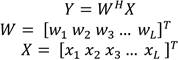 (1)
(1)
in which, W is a complex weight vector, X is the vector of snapshots, L is the number of elements of the ULA and superscripts T, H denote transposition and complex conjugate transposition, respectively.
The snapshot vector and the complex weight vector could be expressed by means of its in-phase (I) and quadrature (Q) components as in (3) and (4) respectively:
X=(I+jQ) e -jwin (3)
W= W I +jW q (4)
where w i is an intermediate digital frequency and n is the sample time. Substituting (3) and (4) in (1) a baseband version of the output is obtained as (5):
Y=(W I I+W q Q)+j(W I Q-W q I) (5)
In order to achieve the IQ components and the conversion to baseband a Digital Down Converter designed in [4] were used. The adaptive algorithm computes the optimal W vector for beamforming.
2.2. -ADAPTIVE LMS ALGORITHM MODEL
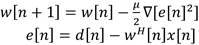
LMS algorithm is a type of no blind algorithm, because it uses a reference signal (RS) for tracking the SOI and steering nulls to the IS. The ASA has to be able to obtain the RS before tracking begins. The systems uses a prior training period to transmit the RS to ASA. LMS minimizes the MSE using an iterative process and upgrades the weight complex vector by moving in the opposite direction of the gradient [3,7], see (6).
 (6)
(6)
where μ is the step-size and e[n] is the error between the output and the reference signal (d[n]). After a mathematical process detailed in [3,7,34] the weight complex vector is upgraded by (7).
w[n+1]=w[n]+μx[n] e * [n] (7)
The step-size controls the convergence of the algorithm. High values of μ produce fast convergence however, the probability of instability grows, the choice of μ is a tradeoff between velocity and stability for what it has to satisfy (8).
 (8)
(8)
Where λ max is the maximum eigenvalue of the incoming signal correlation matrix [34].
3.- SINGLE CHANNEL LMS DESIGN IN SYSTEM GENERATOR
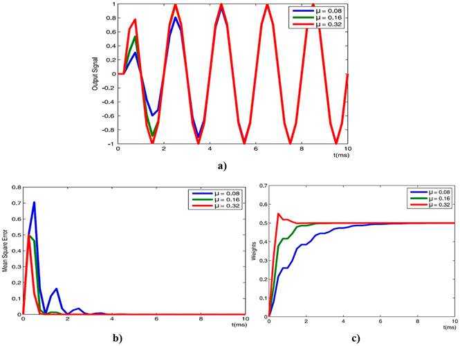
A single channel LMS algorithm is designed using MatLab and System Generator in order to check on FPGA the theory described in section. Figure 4 presents the block diagram of the LMS algorithm.

In and Out blocks are interfaces between MatLab and System Generator. This allows generating input signals for exciting the algorithm and analyzing its response using MatLab. The LMS algorithm is inside of In and Out blocks on system generator environment. Table 1 summarizes the test parameters used.
Table 1 System and signal parameters.
| Parameter | Value |
|---|---|
| Sample frequency ( |
4 kHz |
| Input and Reference frequency ( |
0.5 kHz |
| Input Signal | 2 |
| Reference Signal |
|
Figure 5 exhibits the performance of the LMS algorithm, when the step size is μ=0.08, μ=0.16 and μ=0.32. Figures 5 a) b) validate that μ controls the convergence characteristic of the LMS algorithm. Higher values of μ produce fast convergence. The weights obtained in Figure 5 c) are expected because they tend to the scale factor between reference and input signal (w=0.5).
4.- SPACE TIME ADAPTIVE PROCESSING STRUCTURE
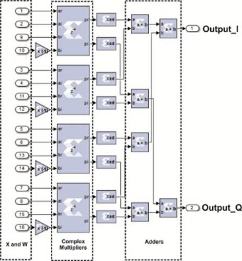
The proposed design in this paper consists in a STAP marked on the Figure 6 with dotted line and in Figure 2. The system is designed using System Generator and MatLab and proven on Xilinx FPGA z7020. In order to highlight, the STAP design has been divided in three functional blocks. The former is a Digital Down Converter (DDC), which has been detailed in [4] and to achieve the IQ components of multichannel signals from an ULA of four elements is used. The second is a digital IQ beamformer, which is able to weight the incoming signal from each array cell using the mentioned IQ components and a complex weight vector. The last block is able to compute this complex weight vector by means of a LMS adaptive algorithm, which has IQ components and reference signal as input signals. Figure 6 presents the block diagram of the proposed system.
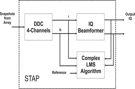
Figure 7 shows the IQ beamformer block. Where IQ components and complex weight vector are input signals. This block use Complex Multiplier 3.0, CMult, Adders and Cast System Generator blocks to achieve the STAP output by means of (5).
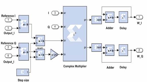
The LMS adaptive algorithm has to be able to process the IQ components and the STAP output for computing a complex weight vector. In order to satisfy the above-mentioned goal a complex LMS Algorithm was implemented, see Figure 8. This LMS design uses Adders, Complex Multiplier 3.0, Cast, Constant and Delay blocks to compute the complex weight vector described by the equation (7)
For analyzing the performance of the proposed STAP, a Quadrature Phase Shift keying (QPSK) transmitter was designed on MatLab environment. Figure 9 depicts the scheme of the transmitter, the propagation channel and the ULA used to generate the snapshots for exciting the designed system.
The transmitter generates the SOI signal by means of a QPSK modulator with gray codification and an Up-Converter, the propagation channel allows adding Additive White Gaussian Noise (AWGN) and interferences or jamming signals, the ULA block simulates an ULA, which computes the snapshots.
The parameters used in snapshots generation are summarized in Table 2.
Table 2 System and signal parameters.
| Parameter | Value |
|---|---|
| data | tag code (0-3) |
| Symbol Rate ( |
2 kbps |
| Sample frequency ( |
4 MHz |
| Intermediate frequency ( |
0.5 MHz |
| Interference Signal |
|
| Interference frequency ( |
507 kHz |
| ULA elements spacing | 0.5 |
| ULA elements | Isotropic |
| step size | 0.004 |
5.- PERFORMANCE ANALYSIS
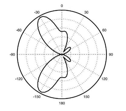
The DDCs used in the proposed design present good performance (BER = 0) processing QPSK signals with signal to noise ratio (SNR) over 5.5 dB. For this reason, the noise power (P n ) is fixed in order to obtain upper values of SNR. The response of the system, to an RFID tag and an interference placed in azimuth angles ϕ soi =-30ο and ϕ soi =60ο respectively, with (A is =0.5) in absence of noise, is shown in Figure 10.
The symbol transitions demand a new convergence of the algorithm, result in glitches and oscillations at the beginning of the symbols. This situation is main in the design of the system because the oscillation time (convergence speed) depend of the step size and the symbol period must be greater than the needed time by the algorithm to converge (T c ). In order to sample at center of the symbol period at the receiver terminal, the system must satisfy the convergence condition T s ≥2T c , where T c is the symbol period.
The step response is shown in Figure 11. The number of samples needed to converge is 300 approximately. The choice of R s , f s and μ must be a tradeoff in order to satisfy the convergence conditions. Figure 12 shows the normalized radiation pattern generated, where the main lobe is steered to SOI and the IS mitigated.

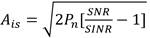
The capacity of the proposed STAP system tracking RFID tags and mitigating interferences is measured in sceneries with different signal to interference plus noise ratios (SINR). In the presented system, the interference amplitude controls the SNIR values for given values of SNR by means of (9).
 (9)
(9)
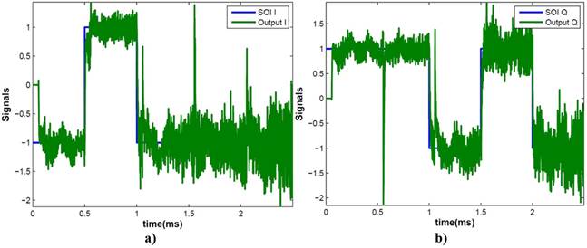
Figure 13 shows the response of the system with SINR = 1 dB and SNR = 7 dB, where noise and accepted interference signal are added to the SOIs in the IQ output signals. Upper levels of interference produce high values of BER in this SNR environment.
6.- RESOURCE CONSUMPTION
The performance of the STAP described in this paper is validated using the co-simulation hardware tool available on System Generator environment. This tool allows generating the VHDL code for Xilinx FPGAs and simulating the system in Software and Hardware at the same time. The results were obtained on Xilinx z7020 platform. Table 3 summarizes the available resources and the resources consumption by the proposed space-time adaptive processing system.
7.- CONCLUSIONS
This paper presents an implementation of a smart antenna processing for RFID applications. Space time adaptive processing with Complex LMS, IQ beamforming and Digital Down Converters is designed for an UHF RFID smart antenna systems. The proposed design in addition of improving the reading range, mitigate interference and reduce the number of readers needed is a simpler design, more robust and lower computational. Furthermore, it has good performance tracking RFID tag signals in environment when information about the incoming signals is known as smart inventory applications. Consumption resources on Xilinx FPGA z7020 allow completing the RFID Reader design on this platform.

