


 Servicios personalizados
 Inglés (pdf)
 Articulo en XML
 Referencias del artículo
 Enviar articulo por email
 Citado por SciELO
  Similares en
SciELO
Similares en
SciELO 
 Permalink
1.- INTRODUCTION
Filtering is essential to process communication signals to improve the quality of the signal of interest. Some major reasons to apply are the need to suppress noise and interference or to discriminate between multiplexed signals [1]. To that end, Linear Time-Variant (LTV) filters are reported to apply in a variety of fields such as control systems [2], communications [3], signal processing, biomedical applications [4] and circuit modeling [5].
Nowadays, several applications requiring filtering operations demand high commutation speed [6], which represents a difficult task to achieve relaying on LTI filters. According to [7], lowpass filtering is characterized by long transient states which introduce distortion that affects the output filtered signal. Filtering operations are limited by LTI systems due to fixed parameters, which entails a relatively large risetime. To derive lower values of risetime, the output filter response is restricted by the uncertain principle. This principle establishes theoretical and practical limits to obtain shorter risetime values and simultaneously to reduce noise when filter parameters are constant in time [8]. To this end, LTV filters are designed to overcome these constraints.
LTV filters perform a variation of internal coefficient values to reduce risetime, then to decrement distortion of the output filtered signal. Several design approaches are based on
Laplace characterization for LTV filters is exposed by [2]. In this paper, the applicability of Laplace transform techniques for LTV filters is demonstrated by developing frequency-domain models applied to basic network elements. This paper establishes main in-out relations over which common LTV filter designs are structured.
Some designs of filters with variable cutoff frequency are not addressed to reduce risetime but to provide several available cutoff frequencies in the same design. A design method for Variable Digital Filters (VDF) is reported in [3]. This method proposes a Finite Impulse Response (FIR) Variable Digital Filter (VDF) described by a piecewise high attenuation function on the stopband. Additionally, the report in [9] employs a single lowpass prototype filter to obtain variable lowpass, highpass, bandpass and bandstop frequency responses. These filters can modify frequency response on-the-fly and represents a low complexity alternative to the other similar design reported in [10].
LTV filters topic is presented by [11] through the definition of Linear Periodic Time Variational (LPTV) filters. A linear filter can be called an LPTV filter of period
Commonly, LTV techniques derive reduction of risetime parameter by synchronously changing coefficients during the transient interval of the filter, i.e. damping factor [7] and instantaneous bandwidth [8]. This approach has been widely used in several designs by stable LTV multi-notch Infinite Impulse Response (IIR) filters [13], IIR multi-notch filters [4] and FIR [14] filters. Typically, instantaneous bandwidth changes according to a heuristic function of time. By these methods, a variety of simulation and obtained results confirmed the advantage over the stationary counterpart LTI filters in terms of reducing the transient period length.
Designing time-variant filters on Field Programmable Gate Array (FPGA) devices is recommendable due to inherent re-programmable characteristics from reconfigurable hardware. By means of FPGA devices, dynamic of parameters is commonly allowed to implement for filtering operations to further improve integration, processing speed and expanding system capabilities. Taking advantage of these features a variety of solutions are reported to devise digital signal processing methods on FPGA. For instance, some recent solutions are reported to FIR filter design by using Stratix II FPGA [15], self-programmable filter on Xilinx FPGA including Embedded Microprocessors [16], FIR filter design subject to energy constraints [17] and smooth filtering of multispectral satellite images [18] to improve quality.
Current work addresses the design of an LTV filter to implement on FPGA devices based on the report in [8], which is inspired in the widely consulted work presented in [19]. Then to carry out several simulations to validate performance. Based on the design exposed by [8] it is expected to preserve, on the proposed digital design, main time restrictions such as risetime and overshoot. The current article is organized as follows: Section 2 describes the digital design and filter implementation on FPGA, Section 3 discusses the main results and concluding remarks are presented in Section 4.
2.- DIGITAL DESIGN OF THE TIME VARIANT FILTER
Similar to LTI filters, the design of LTV filters demands to devise the transfer function, then to implement on a given technology. Current section analyses the reported LTV design of second- and fourth-order systems and the proposed implementation on FPGA.
2.1.- FILTER SPECIFICATIONS DESCRIPTION
Filter specifications are established by a second-order lowpass filter with cutoff frequency
where
Values for
for
The solution to the optimization problem, provided after solving (2), optimally reduce the risetime parameter of the filter output. The sequence for
In practice, to device the second-order system from (1) with the time-varying coefficient

Although the LTV system in (1) with a time-varying coefficient
where values of
2.2.- FILTER IMPLEMENTATION ON FPGA
Current Section proposes the functional implementation on FPGA of a discrete version of the system in Fig. 2, but concatenated in cascade to have a fourth-order system. To this end, blocks of Simulink Xilinx Blockset are employed relaying on System Generator Software (SYSGEN) 12.4. Similar filter designs may be afforded by using this configuration. Fig. 3 exhibits the general scheme to process the input signal, corresponding to that described in [19].
Two main blocks are connected, the Coefficients Update block to conform the time-varying filter coefficients

LTV Filter block is implemented by two identical second-order systems. Fig. 4 depicts the obtaining of one of the second-order systems from the LTV Filter block in Fig. 3. Both of them are structurally identical and are connected in cascade as depicted in Fig. 5, only the coefficient values are different. The implementation of the second-order system in Fig. 4 is a direct discrete representation of the state-variable diagram in Fig. 2. The integrators are implemented by the transfer function
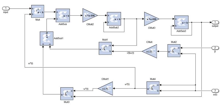

Coefficient Update block provides the time-varying coefficient sequences

The Preprocessing block in Fig. 6 is implemented by using a third-order IIR lowpass filter. The normalized cutoff frequency is equal to the number of samples in a semi period of the binary input signal. This value reduces as much as possible undesirable input noise and preserves main frequency components of the binary signal simultaneously. The coefficients of the IIR lowpass, of the Preprocessing block, were derived by using the software fdatool of Matlab. The filter was implemented by using Direct Form II method as depicted in Fig. 7 [23]. Direct Form II is selected due to the reduction on the total numbers of delay elements. Filter coefficients were exported from fdatool and obtained the structure shown in Fig. 7.

Following the Preprocessing subsystem, the Detection subsystem is implemented as depicted in Fig. 8. To detect when the input signal in “In” intersects the threshold value in “Threshold” a comparator is used by the Relational block. The threshold value is established on

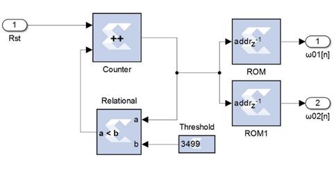
The Coefficients Storage subsystem is implemented as depicted in Fig. 9. Time-varying coefficients are stored on ROM blocks and these are continuously fetched by the Counter block. The Counter block output values ranged from zero to the length of the ROM stored sequence. In case that the counter output value reaches the length of ROM stored sequence, then the counter is disabled by the Relational block. This is needed to avoid overflow to access ROM blocks.
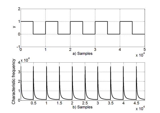
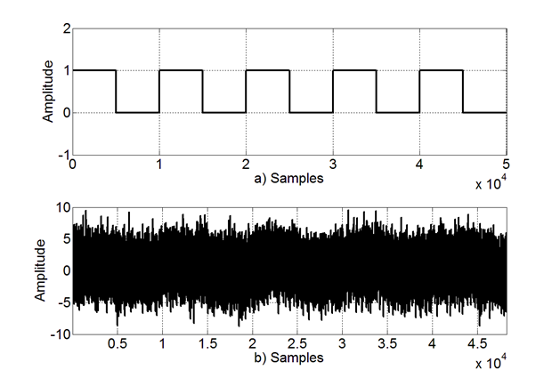
To illustrate the overall functionality of the system in Fig. 6, Fig.10 exhibits signals from the Scope block by Signals A, B, C and D. Based on the noisy binary signal in Fig. 10 a) (Signal A), the preprocessing block reduces noise at the output in Fig. 10 b) (Signal B) by IIR filtering input samples. This is needed to cancel out noise and better detect binary transitions on the received signal. Based on the Preprocessing output Signal B, the detection block outputs ones on the binary transitions of the received signal, this is depicted in Fig. 10 c) (Signal C). Then, Signal C restarts the Coefficients Storage Block to produce Signal D, where the values of the coefficients are restarted on each input signal transition. Fig. 10 d) represents the final output of the system in Fig. 6.
3.- RESULTS
To derive results of the implemented scheme in Fig. 3, main parameters of filter specifications were settled as follows:
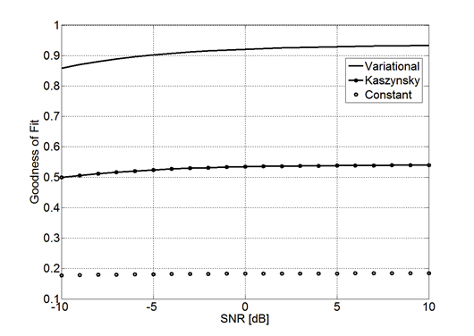
Fig. 12 exhibits results of the implemented system for a variety of design: constant coefficients (LTI), Kaszynsky [7] and the Variational method reported in [8] when Signal to Noise Ratio (SNR) parameter equals to
To measure the quality of filtered signal, Goodness of Fit tests were evaluated. This is calculated using a cost function given by the Normalized mean square error [21]:
Where
The metric in (5) was used to establish a comparison between the ideal input signal represented in Fig. 11 a), and the output filtered signal on the SNR range
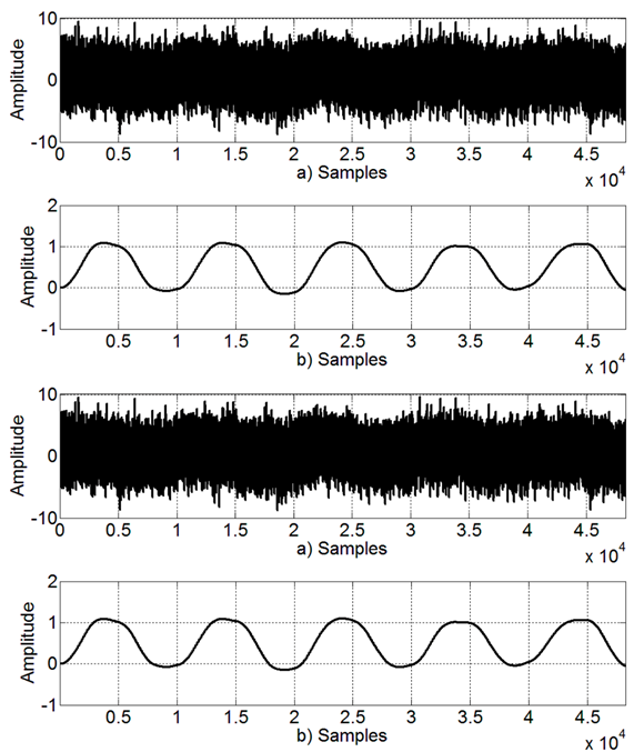
Figure 10 Detection block performance a) Input of Preprocessing block. b) Output of Preprocessing block. c) Output of Detection block. d) Characteristic frequency.

A quick resource estimation needed to build this filter is shown in Table 1. The total number of components is lower than commonly available resources on FPGAs. For instance, on a Spartan3 board with a XC3S500E FPGA device, the occupation percentage of the DSP48A1s is 82%, 22% of the Slices and 52% of the RAMB16BWERs. These occupancy values on FPGA indicate an affordable solution to implement. However, it may be needed an FPGA device with increased features for more complex applications that require the addition of additional intellectual property modules.
4.- CONCLUSIONS
Many modern applications of filters demand the processing of high data rate signals. Under these conditions, it is essential to reduce risetime parameter of filters as much as possible. LTI filters are limited by the constant bandwidth to process signals of shorter time symbol duration. However, LTV filters are reported to circumvent this problem by time-varying coefficients. A design for FPGA implementation of a time-varying parameters filter has been presented in this work. In this case, a fourth-order lowpass filter was designed by Bessel approximant function and using Xilinx System Generator (SYSGEN) software. The proposed design is envisaged to further employ FPGAs capabilities to dynamically reconfigure main parameters. Simulations validated proper performance to reduce risetime parameter and improve the quality of received signal simultaneously. This reduction of risetime parameter allows filtering signals of higher data rates to increase the communication speed. Future work is pointed out to implement an odd filter order and to analyze energy restriction on the proposed design.

