


Mi SciELO
 Servicios personalizados
Servicios Personalizados
Articulo
 Español (pdf)
 Articulo en XML
 Referencias del artículo
 Enviar articulo por email
Indicadores
-
 Citado por SciELO
Links relacionados
-
 Similares en
SciELO
Similares en
SciELO
Compartir

 Permalink
Nucleus
versión impresa ISSN 0864-084X
Nucleus n.41 Ciudad de La Habana ene.-jun. 2007
CIENCIAS NUCLEARES
Calculation of the displacement cross sections and the DPA distribution in hydrogenated amorphous silicon semiconductors detectors in medical digital imaging applications
Cálculo de la sección transversal de desplazamiento y la distribución de los DPA
en detectores semiconductores de silicio amorfo hidrogenado en aplicaciones
de imagenología digital médica
Antonio Leyva Fabelo, Ibrahin Piñera Hernández, Katerin Shtejer Díaz, Yamiel Abreu Alfonso, Carlos Manuel Cruz Inclán
Centro de Aplicaciones Tecnológicas y Desarrollo Nuclear (CEADEN)
Calle 30 No 502 e/ 5ta Ave. y 7ma. Playa, Ciudad de La Habana, Cuba
aleyva@ceaden.edu.cu
ABSTRACT
In present paper the dependence of the displacement cross sections of the different species of atoms in the a-Si:H structure, with the energy of the secondary electrons generated by the X-rays of the typical energies using in medical imaging applications, was calculated using the Mott-McKinley-Feshbach approach. It was verified that for electron energies higher than 1.52 keV it is possible the occurrence of hydrogen atoms displacements, while for the silicon atoms the threshold energy is 126 keV. These results were compared with those obtained for similar detectors but developed with crystalline silicon. With the use of the mathematical simulation of the radiation transport in the matter, the energy spectrum of the secondary electrons was calculated in order to estimate the number of atomic displacements, which take place in the semiconducting amorphous device in working regime.
The spatial distribution of the dpa in the detectors volume, as well as its behavior with the depth in the
work region are presented and discussed in the text.
RESUMEN
Utilizando la aproximación de Mott-McKinley-Feshbach en el trabajo se calculó la dependencia de la sección transversal de desplazamiento para cada especie de átomo de la estructura del a-Si:H en los intervalos de energía típicos de los electrones secundarios generados por los rayos X empleados en aplicaciones de imagenología médica. Se observó que para energías de los electrones superiores a 1,52 keV son posibles los desplazamientos de átomos de hidrógeno, mientras que la energía umbral de desplazamiento de los átomos de silicio resultó de 126 keV. Estos resultados se compararon con los obtenidos para detectores similares pero fabricados de silicio cristalino. Con el empleo de la simulación matemática del transporte de la radiación en la materia se calculó el especto energético de los electrones secundarios con el objetivo de estimar el número de desplazamientos por átomos que tienen lugar en el dispositivo amorfo semiconductor en régimen de trabajo. La distribución espacial de
los dpa en el volumen del detector, así como su comportamiento con la profundidad son presentados
y discutidos en el texto.
Key words: cross sections, atomic displacements, semiconductor detectors, simulation, amorphous
states, silicon, x radiation, images
INTRODUCTION
The use of radiation detectors manufactured with hydrogenated amorphous silicon extends quickly in many fields of science and technology, because its low production cost, the possibility to grow large areas, its appropriate sensibility operating at high temperatures and the possibility to grown thin layers directly over the read-out electronics.
Another of their most important advantages over the crystalline detectors, is the existent compatibility between the characteristics of their structure and the radiacional damage [1], question of maximum importance when the application requires of high operation stability, still after high exposition dose, like it happens in the experiments
of high energies physics and in the medical radiology.
The radiacional damage can be characterized through the quantity of atomic displacements (dpa) of certain atoms specie. For photons irradiation this type of damage can only be produced in an indirect way by means of the secondary electrons that are generated after the primary interactions of the radiation with the matter (photoeffect).
The range of energies for most of the medical digital radiology applications is among some few eV until the 150 keV, although in some applications like mammography and angiography the maximum energy doesn’t exceed the 50 keV.
These relatively low energies are the employees in this paper to determine the X rays effects on the structure of the pin hydrogenated amorphous silicon (a-Si:H) detectors in applications of radiological diagnosis.
Determination of the displacement cross section
The determination of the displacement per atom (dpa) cross section ![]() is an indispensable step to determine of the radiacional damage. Knowing
is an indispensable step to determine of the radiacional damage. Knowing ![]() and the energies spectrum of the particles flow is possible to calculate the total number of atoms that can be displaced of its positions per unit fluence per a target atom. The approach of Mott-McKinley-Feshbach [2] has been used for the
and the energies spectrum of the particles flow is possible to calculate the total number of atoms that can be displaced of its positions per unit fluence per a target atom. The approach of Mott-McKinley-Feshbach [2] has been used for the ![]() calculation. This approach supposes that the atom is bonded to the material with an energy
calculation. This approach supposes that the atom is bonded to the material with an energy ![]() , and for electrons incident energies smaller than
, and for electrons incident energies smaller than ![]() ,
, ![]() = 0, while for the contrary case it is determined by:
= 0, while for the contrary case it is determined by:
where Z is the atomic number of target atom, ![]() - the Bohr radius,
- the Bohr radius, ![]() - Rydberg energy,
- Rydberg energy, ![]() = Z/137,
= Z/137, ![]() - ratio of electron velocity to light velocity,
- ratio of electron velocity to light velocity, ![]() - maximum kinetic energy of recoil atom, M - mass of target atom, m - mass of electron, and
- maximum kinetic energy of recoil atom, M - mass of target atom, m - mass of electron, and ![]() - displacement energy.
- displacement energy.
This approach has been considered exact with a margin of error of 1% for Z ![]() 40 [3].
40 [3].
In Ec. (1) all the parameters are known, with the exception of the displacement threshold energy of the target atom in the structure of the material,![]() .
.
For the case of the a-Si:H the values of ![]() appear in the literature with certain dispersion. For example, in [4] it is reported that for the hydrogen,
appear in the literature with certain dispersion. For example, in [4] it is reported that for the hydrogen, ![]() Ed H = 3.4 eV, in [5] Ed H = 3.3 eV and in [6]
Ed H = 3.4 eV, in [5] Ed H = 3.3 eV and in [6] ![]() = 3.6 eV. The authors of [7] assume that the displacement threshold energy of Si is 20 eV, while in [8] they take
= 3.6 eV. The authors of [7] assume that the displacement threshold energy of Si is 20 eV, while in [8] they take ![]() = 22 eV and in [9] they report that the energy required to remove a silicon atom that is bonded with three other silicon atoms is approximately 25 eV.
= 22 eV and in [9] they report that the energy required to remove a silicon atom that is bonded with three other silicon atoms is approximately 25 eV.
We use ![]() = 3.3 eV taking into account that this value is reported as the bonding energy of H to the Si in the a-Si:H structure and for monovalent atoms the cohesive energy coincides with the displacement threshold energy [10]. For the case of the silicon we use
= 3.3 eV taking into account that this value is reported as the bonding energy of H to the Si in the a-Si:H structure and for monovalent atoms the cohesive energy coincides with the displacement threshold energy [10]. For the case of the silicon we use ![]() = 22 eV, an average of the reported values.
= 22 eV, an average of the reported values.
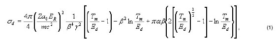
The figures 1 and 2 show the founded dependences for the displacement cross-sections for hydrogen and silicon atoms respectively, with the electrons and positrons energy.
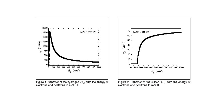
The analysis of both figures show that, in our experimental conditions (![]() < 50 keV, typical maximum energy in the most of medical radiographic applications) the probability of H atoms of being displaced from their position is nonzero only for energies higher than 1.52 keV, while the Si atoms are insensitive to the displacement effects because to achieve its displacement from the bonded position there are required electrons with
< 50 keV, typical maximum energy in the most of medical radiographic applications) the probability of H atoms of being displaced from their position is nonzero only for energies higher than 1.52 keV, while the Si atoms are insensitive to the displacement effects because to achieve its displacement from the bonded position there are required electrons with ![]()
![]() 126 keV. This result allows concluding that in the a-Si:H detector the structural displacement defects are only possible for the hydrogen atoms that passivate the dangling silicon bonds.
126 keV. This result allows concluding that in the a-Si:H detector the structural displacement defects are only possible for the hydrogen atoms that passivate the dangling silicon bonds.
For c-Si the ![]() was also calculated using the same code and
was also calculated using the same code and ![]() = 25 eV reported in [11,12]. Figure 3 shows the
= 25 eV reported in [11,12]. Figure 3 shows the ![]() behaviour with the electron energy in this crystalline material. As is observed, the differences between the calculated results for a-Si:H and c-Si are very small, because of the similar displacement threshold energy. For example, in [13] was reported that the d s for silicon in c-Si irradiated with 1 MeV electrons is 68 barn, while for identical energy our results were 70.3 barn for the same material and 67.2 barn for hydrogenated amorphous silicon. Also, the displacement threshold energies for silicon in c-Si reported in the literature, 133 keV [14] and 150 keV [15], are very close to our results, 126 keV for a-Si:H and 141 keV for c-Si.
behaviour with the electron energy in this crystalline material. As is observed, the differences between the calculated results for a-Si:H and c-Si are very small, because of the similar displacement threshold energy. For example, in [13] was reported that the d s for silicon in c-Si irradiated with 1 MeV electrons is 68 barn, while for identical energy our results were 70.3 barn for the same material and 67.2 barn for hydrogenated amorphous silicon. Also, the displacement threshold energies for silicon in c-Si reported in the literature, 133 keV [14] and 150 keV [15], are very close to our results, 126 keV for a-Si:H and 141 keV for c-Si.

Hydrogen dpa determination
Having the values of ![]() as a function of the secondary electrons energy, to calculate the dpa, it is required to determine the energy spectrum of the secondary electrons in the volume of interest.
as a function of the secondary electrons energy, to calculate the dpa, it is required to determine the energy spectrum of the secondary electrons in the volume of interest.
To calculate this flow spectrum the code system MCNP-4C [16] based on Monte Carlo method was employed. MCNP-4C simulates the transport of photons and electrons in matter.
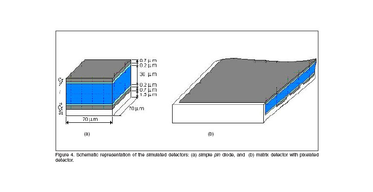
In the simulation were taken into account all material and geometric details of both detectors (simple pin detector and matrix detector based in pin diode with pixelated electrode, figures 4(a) and 4(b) [17]).
As X-rays source, a parallel photons beam generator with the Mo emission spectrum (17.6 keV and 19.7 keV) was modeled.
The distance between the source and the detector was selected l = 60 cm. The histories numbers for each experiment was selected according to the required statistic. In all the cases the relative error of the calculated values was lower than 10%. The results of simulation were obtained using the tally F4, which deliver the values of the differential energy flow in (![]() ).
).
This spectrum is multiplied by the corresponding cross sections and integrated in the interesting energies interval, determining by this way the total number of dpa that take place as consequence of the transport in the device of each incident photon.
When irradiating the detector with photons coming from the Mo source (![]() photons) it is observed that the distribution of the calculated atomic displacements in the intrinsic layer as a function of the depth presents a behavior, just as it is shown in figure 5.
photons) it is observed that the distribution of the calculated atomic displacements in the intrinsic layer as a function of the depth presents a behavior, just as it is shown in figure 5.
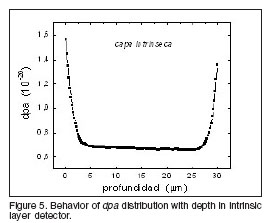
The obtained distribution is characterized by very high values of dpa in the adjacent regions to the Cr electrodes, as a consequence of the higher Z of Cr with respect to the Z of the intrinsic material, which lead to the increment of the number of generated secondary photoelectrons ![]() particles with the ability to provoke atomic displacement on the hydrogen atoms.
particles with the ability to provoke atomic displacement on the hydrogen atoms.
The highest value of dpa is reached near the front surface, 1.56 x ![]() , while in the center of the active intrinsic volume the number of dpa is 6.65 x 10⁻²¹. It means that for each
, while in the center of the active intrinsic volume the number of dpa is 6.65 x 10⁻²¹. It means that for each ![]() -
-![]() photons that impact in the sensor of 70x70x30
photons that impact in the sensor of 70x70x30 ![]() only will take place between 1 and 7 hydrogen atomic displacements.
only will take place between 1 and 7 hydrogen atomic displacements.
This number of structural defects is very small and completely negligible keeping in mind that the average number of photons incident in a similar detector working in conditions of clinical operation in one year is ~ 1 x ![]() . This annual number of photons was calculated using the data of deposited dose (2 x
. This annual number of photons was calculated using the data of deposited dose (2 x ![]() Gy) reported in [18] in a similar detector.
Gy) reported in [18] in a similar detector.
By the same way, using in the calculation the dose data reported [19], the maximum number of photons that impact in our detector under real diagnostic exploitation in one year doesn’t exceed the ![]() photons, still smaller value.
photons, still smaller value.
Besides this, some authors, as example [20, 21], demonstrate experimentally that in a-Si:H the recombination processes of defects are very improved thanks to the characteristics of the own structure. This natural process contributes, as these authors report, to the reversion of the generated defects by the recombination simply by a 5-10 h room temperature annealing.
Previous experimental studies [18, 22] demonstrated that these low dose levels do not have a significant effect in the values of the carrier mobility, linearity and other noise properties in a-Si:H detectors or FET. This way they conclude that the devices based on the a-Si:H has the appropriate and necessary resistance to the radiacional damages indispensable for these applications.
In the case of the a-Si:H matrix detector, given their large dimensions, the calculation shows a higher dispersion of the results although 2.5 x ![]() histories were run. Nevertheless the relative error stayed inferior to 10%.
histories were run. Nevertheless the relative error stayed inferior to 10%.
The figure 6 shows the obtained results for the dpa distribution in the intrinsic volume of three different pixels (lateral, corner and a center) as a function of the depth. Observe the same behavior that in the figure 5 with very little difference relative to the position that occupies the pixel in the matrix arrangement.

CONCLUSIONS
Using the Mott-McKinley-Feshbach approach the displacement cross sections of H and Si in a-Si:H were calculated as a function of the secondary electrons energy. It was determined that the probability of occurrence of hydrogen atoms displacements from the structure is possible for energy superiors to the 1.52 keV, while for the silicon atoms it is possible for energies that surpass the 126 keV.
The number of defects generated as consequence of the H atoms displacements, according to the calculation, is totally negligible in order to affect the efficient work of the device under operation conditions.
These results, supported by the reports about the amplified defects recombination properties of this material and the effective and fast restoration of the radioinduced damages after the device annealing at room temperature, contribute to support the idea that the devices based on the a-Si:H have the appropriate and necessary resistance to the radiacional damages, indispensable for the applications of digital medical radiology.
REFERENCES
[1] MOARES D. Advance solid state detector Technology for particle detection. 10th Workshop on Electronics for LHC and Future Experiments. Boston, 2004. 13-17 September.
[2] MCKINLEY WA, FESHBACH H. Phys. Rev. 1948; 74: 1759.
[3] CURR RM. Proc. Phys. Soc. A. 1955; 68: 156.
[4] TAKAHASHI M, KONAGAI M. Amorphous Silicon Solar Cells. London: North Oxford Academic Publisher Ltd, 1986.
[5] WEAST RC. Handbook of Chemistry and Physics. Boca Raton: Chemical Rubber Corp, 1998.
[6] KOSTESKI T. Tritiated Amorphous Silicon Films and Devices. Thesis for the degree of Doctor of Philosophy. University of Toronto. 2001.
[7] VAN SWAAIJ RACMM, ANNIS AD, SEALY BJ. J. Appl. Phys. 1997; 82 (10): 4800-4804.
[8] WEHRSPOHN RB, DEANE SC, FRENCH ID, et al. J. Appl. Phys. 2000; 87 (11): 144-154.
[9] SCHNEIDER U, SCHODER B. Amorphous Silicon and Related Materials. Singapore: World Scientific, 1988.
[10] MOLLER W. Appl Phys A. 1993; 56: 527.
[11] HACKLER WA, KIKUCHI CH. Study of Lituium mobility in ittadiated silicon. Technical Report ORA Project 04381, NASA. 1966.
[12] HIRAIWA A, KOBAYASHI T. J. Appl. Phys. 1991; 70: 309.
[13] TADA HY, CARTER JR, ANSPAUGH JRBE, DOWNING RG. Solar Cell Radiation. Handbook. Third Edition. JPL Publication, 1982; 82-69.
[14] HAN M, BENNETT JC, ZHANG Q, et al. Thin Solid Films. 2006; 514: 58-62.
[15] SUMMERS A, et al. Trans Nucl Sci. 1993;( 40): 1372.
[16] SUMMERS A, et al. Trans Nucl Sci. 1993;( 40): 1372. B
[17] LEYVA A. Informe Técnico de la Salida contratada en octubre de 2005. PRN/7-2/11. AENTA. 2005.
[18] BOUDRY LM, ANTONUK LE. Med. Phys. 1996; 23 (5): 743-753.
[19] ROHR P. Amorphous silicon based matrix detectors for X-ray Imaging. User Meeting Workshop. ESRF. Grenoble, Febrary 2003.
[20] SHIMIZU T, MAEHARA T, MASAHIRO M, et al. Jpn.J.Appl.Phys. 2001; 40: 1244-1245.
[21] IMAGAWA O, YASUDA K, YOSHIDA A. Jpn. J. Appl. Phys. 1989; 66 (10): 4719-4722.
[22] ANTONUK LE, BOUDRY LM, YORKSTON J, et al. Nucl. Inst. Meth. A. 1990; 299: 143-146.
Recidido: 14 de abril de 2007
Aceptado: 28 de mayo de 2007
