


 Custom services
 English (pdf)
 Article in xml format
 Article references
 Send this article by e-mail
 Cited by SciELO
  Similars in
SciELO
Similars in
SciELO 
 Permalink
Introduction
The chromium compensated gallium arsenide (GaAs:Cr) is attaining a relevant position among the materials devoted to the development and fabrication of radiation detectors due to its high resistance to the radiation damage, high effective Z, relative low production cost, possibility to grow large area crystals, etc. [1].
The production process of this novel material has been developed and optimized at the Tomsk State University, Russia [2]. With its use, some devices have been developed for radiation detection, such as hybrid detectors with Timepix readout electronics based on the GaAs:Cr [3-4]. This detector has been used in, for example, the construction of a microtomograph for biological and geological studies [5]. But, given the aforementioned properties of the sensitive material, it is expected to become indispensable in High Energy Physics research .
The studies that take the GaAs:Cr as target continue advancing, deepening in the knowledge of its properties and its behavior in different exploitation regimes, seeking also to enhance some of its most outstanding characteristics, such as the radiation hardness.
To undertake the research, the mathematical simulation of the radiation transport in materials is used as a complementary tool, allowing to obtain useful information to interpret experimental results, to predict behaviors, optimize experiments, calculate radiation damage, etc.
Different commercial and own code systems, all based on Monte Carlo method, have been used for this purpose and this paper aims at presenting some of the first most outstanding results that we have obtained.
Materials and methods
The Timepix hybrid pixel detector based on chromium compensated gallium arsenide is shown in figure 1 (a), where the source position and the radiation direction respect to the sensor have been drawn. Although in this figure the direction of incidence is perpendicular, this angle was changed within a wide range to satisfy certain work conditions. The GaAs:Cr thickness was in interval 300 - 900 µm, the pixel area 45x45 µm2 and the pitch 55 µm. figure 1(b) shows the representation of a pixel with its main components and dimensions.
All these sensor characteristics and the particularities of each individual experiment were taken into account in the correspondent simulations.
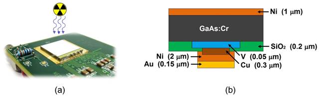
Figure 1 Photograph of the hybrid detector where the location of the radiation source and the photons and particles direction are drawn (a), and graphic representation of a detector pixel with its main components and their dimensions (b).
In order to determine the spatial distribution of the energy deposited by the electrons and photons in the sensor the MCNPX code was used [6]. This is a general-purpose Monte Carlo radiation transport code with three-dimensional geometry and continuous-energy transport of 34 particles and light ions. MCNPX also provides or shows directly the flux energy distribution, separating contributions from electrons and positrons, which is essential in this work for subsequent calculations of radiation damage.
The EGS4 code system [7] was used specifically to determine the shape and other characteristics of the charge carriers cloud generated around the photon or particle interaction point.
The collection of software packages SRIM [8], which calculate many features of the ions transport in matter, were employed in order to determine the energy loss of 22Ne ions and its distribution inside the sensor, the ion stopping powers, the range and straggling distributions and others parameters related to collision events.
The relative errors of all simulation results were always below 3%, which was achieved by running a large number of stories (> 1x10⁷).
Finally, the MCCM code system was used to calculate, following the classical methodology described in [9], the atomic displacement cross sections (( dpa ), as well as the number of displacements per atom (dpa) generated in the irradiated material for different experimental conditions. For determining dpa, the results related to the flux energy distribution inside the target material obtained from MCNPX were used by MCCM.
Since there is no information in literature about the displacement threshold energyvalues (T d ) in GaAs:Cr, its selection was made taking into account the data reported by literature for GaAs, see for example[10-14], and the particularities of our target. Thus, the following thresholds were selected: T d Ga = T d Cr = 10 eV, y T d As = 15.5 eV.
Discussion and results
For a 900 µmGaAs:Cr detector, the in-depth profiles of the deposited energy for different photon energies calculated with the MCNPX are shown in figure 2. Each E dep value presented in this figure corresponds to the energy amount deposited in a 5 μm thickness, layer, which is the width of layers (perpendicular to the photon incidence direction parallel) in which the detector was divided for the calculation. The E dep values in the main regions crossed by photons in their movement from the source to the anodes (data extracted from these behaviors), and other interesting data are presented in table I.
Table I Calculated values for the mass attenuation coefficients and mean free paths in GaAs:Cr, and the deposited energies in different detector regions.
|
|
|
|
|
|
|
|---|---|---|---|---|---|
| 13.9 | 112.4 | 16.73 | 0.049 | 0.931 | 12.53 |
| 17.48 | 61.30 | 30.67 | 0.025 | 0.622 | 16.84 |
| 26.34 | 20.03 | 90.88 | 0.013 | 0.252 | 25.42 |
| 59.54 | 2.085 | 901.95 | 0.009 | 0.031 | 33.69 |
(* - the photon source was placed at 30 cm on the detector surface)
As it can be seen, the highest energy values are deposited precisely in the detector active zone. For the three lowest photon energies the E dep in the GaAs:Cr is greater than 90% of the initial energy. Only for 59.54 keV photons this percentage is lower as a consequence of its high penetration ability. Table I shows that the mean free path of these photons is slightly greater than the detector thickness.
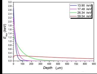
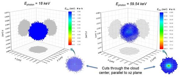
Figure 3 The shapes and dimensions of the generated charges clouds around the interaction point in GaAs: Cr for two photon energies.
A detailed profile analysis for 59.54 keV photons shows that in the detector active zone its behavior leaves the regular exponential decay in the regions near the limits with the electrodes (20 - 25 microns). This phenomenon is associated with the existing differences between the effective Z of the two-adjacent media, taking into account the strong dependence of the interaction processes of this parameter.This dependence and the contribution of backscatter effects can produce the observed behavior. For 26.34 keV photons, a similar behavior was also observed in the region near the Ni cathode, although much less marked.
From the calculated deposited energy, it is possible to determine the number of generated charge carriers dividing the E dep value by the energy needed to create an electron-hole pair in the material (4.184 eV for GaAs:Cr). By doing so, it is possible to estimate not only the generated charge carriers number, but also their spatial distribution.
Figure 3 presents the shape of the charge carriers clouds generated in the medium around the photon interaction point for two different photon energyvalues. These clouds were calculated with the GEANT4 code which makes easier to force photons to interact at a selected point. The obtained results reveal the spherical like shape of clouds and allow determining its average diameter and the internal charge distribution. Additionally, after a complementary processing, these results also allow to calculate the total charge induced in the detector electrodes, the shape and duration of the induced signal, and give the possibility to study the sharing effects between the detector pixels, etc.
The SRIM code system [13] was used to simulate an experiment performed in one of the U400M cyclotron output channels of the JINR Flerov Laboratory of Nuclear Reaction, where 22Ne ions were accelerated to energies 77 and 158.4 MeV. The ion ranges calculated with the program for these energies was 26.3 μm and 73.3 μm respectively.
As an example, Figure 4 graphically presents the results obtained for 158.4 MeV 22Ne ions. In them it can be verified, for example, that 22Ne ions reach to deposit all their energies inside the 300 μm GaAs:Cr sensor, and that the losses by ionization are still the dominant processes.More than 99.7% of the deposited energy is lost in processes associated with the ionization, and only at 0.3% is related to recoil events. The in-depth distribution of the produced vacancies is also showed.
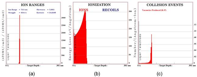
Figure 4 In-depth distributions of stopped ions (a), energy loss (b), and produced vacancies (c), in 300 µmGaAs:Cr for 158.4 MeV 22Ne ions.

Using the MCCM code the displacement per atom cross sections σ( dpa ) for the electrons and positrons in the target material were calculated for energies up to 25 MeV. Figure 5 shows the calculation results of the total σ dpa for each atom specie in the GaAs:Cr for the selected T d set. The particle energy for which the dpa cascade processes begin are distinguishable in the σ dpa graph as the point where the curve abruptly changes its behavior. Detailed analysis of the results shown in figure 5 at low energies shows that multiple displacements occur for electron kinetic energies higher than about 1.15 MeV for Ga atoms, 1.57 MeV for As atoms and 0.93 MeV for Cr.
As it was expected, the displacement cross sectionsfor each atom vanish below a certain incident particle energy, and this value is precisely the minimum kinetic energies necessary for displacing the atoms with determined T d . The presented results allow estimating these cutoff values: 256 keV for Ga, 377 keV for As and 200 keV for Cr.
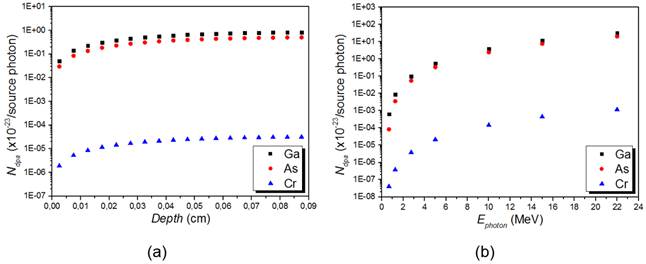
Figure 6 In-depth distribution of the generated dpa number in 900 µm GaAs:Cr irradiated with 5 MeV photons (a), and the behavior of the generated dpa number in GaAs:Cr with the photon energy (b), for each atom species.
By means of the secondary particles energy fluxes calculated with the MCNPX for 900 µm GaAs:Cr detector, the distribution of the dpa number can be determined with the MCCM code, as shown in the example of figure 6(a) for 5 MeV incident photons. Here, the N dpa behaviors with the depth for all the atom species show increasing profiles throughout the thickness of the material, but reveal in Ga certain attenuation with the depth.The very low values of atomic displacements per source photon obtained for Cr are due to the fact that the percentage of Cr atoms present in the target is 0.0023, when for Ga and As atoms are 49.9989.
The calculations made with the MCCM for different incident photon energies give the possibility of obtaining the N dpa vs. photon energy behaviors presented in Figure 6(b) for each atom type. These calculated dependencies show that the N dpa profiles increase with the photon energy, as expected. It stands out that as energy increases, the numbers of dpa corresponding to Ga and As atoms approach each other.
Conclusions
Using a code systems set based on the Monte Carlo method for the simulation of the radiation transport and the radiation damage in matter, some Timepix hybrid detectors based on GaAs:Cr in several configurations were studied.For a 900 µm detector the calculated in-depth E dep profiles for different incident photon energies show that the highest energy values are deposited in the detector active zone. For the three lowest studied energies the E dep in this region are greater than 90% of the initial photon energy, and only for 59.54 keV photons this percentage is lower as a consequence of its larger penetration power. For some energies, it was observed that in the electrode vicinities the profiles showed irregularities that were associated with the existing remarked differences between the effective Z of the two-adjacent media. The shape, dimensions and internal charge distribution of the clouds generated around the interaction point for two photon energy values were determined. For 77 and 158.4 MeV 22Ne ions the ranges in GaAs:Cr were calculated, being 26.3 μm and 73.3 μm respectively. It was verified that 22Ne ions reach to deposit all their energies inside the active 300 µm detector zone, and the losses by ionization are the dominant processes. The σ dpa for GaAs:Cr were calculated for energy values up to 25 MeV, allowing to determine that multiple displacement processes take place for electron kinetic energies higher than 1.15 MeV for Ga, 1.57 MeV for As and 0.93 MeV for Cratoms. The kinetic energies needed to displace atoms in the target were estimated in 256 keV for Ga, 377 keV for As and 200 keV for Cr atoms. In a 900 µm GaAs:Cr detector the in-depth distributions of the N dpa for each atomic species show increasing profiles throughout the thickness of the material, revealing a certain attenuation with depth.The N dpa vs. photon energy behavior show increasing profiles for the three elements present in the material, standing out that with energy growth, the numbers of dpa corresponding to Ga and As atoms approach each other.

