


My SciELO
 Custom services
Services on Demand
Article
 English (pdf)
 Article in xml format
 Article references
 Send this article by e-mail
Indicators
-
 Cited by SciELO
Related links
-
 Similars in
SciELO
Similars in
SciELO
Share

 Permalink
Ingeniería Electrónica, Automática y Comunicaciones
On-line version ISSN 1815-5928
EAC vol.38 no.2 La Habana May.-Aug. 2017
ORIGINAL PAPER
An approach to the numerical solution of one-dimensional heat equation on SoC FPGA
Computación con esténcil para la aproximación a la solución numérica de la ecuación de calor sobre SoC FPGA
Luis Castaño, Gustavo Osorio
Facultad de Ingeniería y Arquitectura, Universidad Nacional de Colombia, Manizales, Colombia.
ABSTRACT
A common kernel used in scientific computing is the stencil computation. FPGA based heterogeneous systems has been used to overcome stencil algorithm performance limitations due to the memory bandwidth on CPU and GPU based systems. Performance improvement is achieved through the combination of several data flow optimization techniques, taking advantage of the FPGA inherent parallelism. However, array architectures used for some two-dimensional problems involves the need of considerable number of FPGAs, for mesh sizes that can be treated by a CPU or GPU based system with a suitable performance at a lower cost. With the development of high level synthesis tools, the implementation of algorithms over FPGA is performed with a better design flow than traditional logic design. In this case, optimization techniques are performed at software level. In this document is presented a system designed to evaluate the performance of a stencil computation algorithm over a SoC FPGA at hardware level. The data-path is designed to perform the stencil computation algorithm using a one-dimensional array of processing elements and registers. System performance is evaluated for the approach to the numerical solution of a heat transfer problem modeled with the heat equation for the one-dimensional case. The proposed architectures are implemented in a ZedBoard Zynq Evaluation and Development Kit using Vivado Design Suite and Xilinx SDK.
Key words: FPGA, stencil computation, heat equation, finite differences
RESUMEN
La computación con esténcil es un esquema muy usado en la computación científica. Se han desarrollado sistemas heterogéneos basados en FPGA para superar las limitaciones debidas al ancho de banda de memoria en los sistemas computacionales basados en CPU o GPU. El mejoramiento del desempeño es logrado mediante el uso de varias técnicas de optimización del flujo de datos, tomando ventaja del paralelismo inherente de los FPGA. Sin embargo, las arquitecturas usadas en problemas bidimensionales involucran el uso de una cantidad considerable de FPGA, para tamaños de malla que pueden ser procesados en sistemas basados en CPU o GPU con un desempeño aceptable a menor costo. Con el desarrollo de herramientas de diseño de alto nivel, la implementación de algoritmos sobre FPGA es realizada con un mejor flujo de diseño que con el diseño lógico tradicional. En este caso las técnicas de optimización se desarrollan a nivel de software. En este documento se presenta un sistema diseñado para evaluar el desempeño de la computación con esténcil sobre una FPGA a nivel de hardware. El camino de datos es diseñado para el empleo de un arreglo unidimensional de elementos de proceso y registros para reducir el número de operaciones de transferencia de datos de memoria. El desempeño del sistema es evaluado para la aproximación a la solución numérica de un problema de transferencia de calor, modelado con la ecuación de calor para el caso unidimensional. Las arquitecturas propuestas son implementadas sobre una ZedBoard empleando Vivado y el Xilinx SDK.
Palabras claves: FPGA, computación con esténcil, ecuación de calor, diferencias finitas
1.- INTRODUCTION
A common kernel used in scientific computing is the stencil computation, particularly for linear algebra algorithms, partial differential equations (PDE) and image processing. It is efficient for the approach to the numerical solution of PDE using the explicit finite difference scheme [10]. However, performance of algorithms based on stencil is limited by the difference between the maximum throughput and maximum bandwidth memory on multi-core CPU and GPU based systems [3]. For this reason, the study of stencil algorithms implementation and optimization methods has been of interest. Cache based optimization techniques have been developed for CPU or GPU based systems to overcome the performance limitations by exploiting the temporal and spatial locality, as can be found in [5, 6, 9, 11]. However, there are performance limitations that remain despite the use of optimization methods [3].
For this reason, FPGA-based accelerators are used as an alternative given that these devices have shown better performance with lower power consumption [1, 2]. The performance improvement of the stencil computing scheme using FPGAs is study in [1, 3, 4, 7, 8]. FPGA based systems take advantage of the inherent parallelism for performance improvement through the combination of several data flow optimization techniques. For instance, grid array architectures as proposed in [3, 7] use streaming and pipeline to accelerate stencil computation. However, the use of such architectures involves the need of considerable number of FPGAs to simulate problems with mesh sizes that can be treated by a CPU or GPU with suitable performance at a lower cost.
The use of FPGA based system has always represented multiple challenge from the number representations to the design flow complexity. The recent development of design tools has allowed overcoming many of these challenges. In [1] Schmitt et al. demonstrate the feasibility to deal with a stencil computation for a grid of 4096×4096 on a single FPGA using a High-Level Synthesis (HLS) tool for system design. In this case, optimization techniques are performed at software level.
In this work, we present a hardware level implementation and optimization of a stencil algorithm on an SoC FPGA. A custom IP for the programmable logic (PL) section interacts with an ARM core that acts as a host processor. System performance is evaluated for the approach to numerical solution of the one-dimensional heat equation over a single FPGA. A baseline architecture use a stencil kernel as the processing element (PE) and a control unit performs the sequence of the stencil algorithm. For system parallelization is developed a data-path with a one-dimensional array of processing elements with feedback through a registers bank, with the aim to reduce the resources utilization and memory transfer operations. System analysis shows the performance achieved in terms of the processing time for the stencil algorithm with four implemented architectures. The processing time is compared with the obtained with the sequential algorithm written in C running over one of the ARM CORTEX A9 core of the SoC FPGA. Problem and system description are detailed in sections 2 and 3 respectively. Numerical results and performance analysis are presented in sections 4 and 5. Finally conclusions and future work are drawn in section 6.
2.- PROBLEM DESCRIPTION
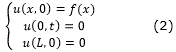
Consider the PDE shown in (1).
This expression represents a 1D parabolic PDE which is used to model the heat distribution over time in a bar with length L. Given an initial value and boundary conditions problem as shown in (2), equation solution shows the temperature variation in the space-time domain.
An approach to the numerical solution of this equation is obtained using the explicit finite difference method. Defining J and N as the number of points for discretization in the space and time domain respectively, the approximate solution is obtained using (3). From this expression, a stencil kernel circuit is obtained as shown in Figure 1.
This kernel is used to calculate each one of the mesh points as shown in Algorithm 1.
Algorithm 1. Pseudo-code for the stencil computation to obtain the approach to the numerical solution of heat equation with the explicit scheme.
for n from 0 to N-1 do
for j from 1 to J-2 do
![]()
end for
end for

In this work is presented the use of the Algorithmic State Machine (ASM) method for the logic design at Register Transfer Level (RTL) of a circuit that performs the stencil algorithm on a SoC FPGA. Variations of the data path are made to evaluate the improvement of the system performance.
3.- SYSTEM DESCRIPTION
The system is implemented in a ZedBoard Zynq Evaluation and Development Kit using Vivado Design Suite. The design takes advantage of the XC7Z020CLG484-1 Xilinx SoC FPGA architecture. The ZYNQ-7 processing system (PS) for the ARM Cortex -A9 MPCore interacts with a custom IP created for the programmable logic (PL) section. The system block diagram is shown in Figure 2.
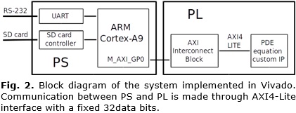
The ARM core acts as the host processor where the main application runs. The custom IP is used to obtain the approach to the numerical solution of the PDE using the stencil scheme. The custom IP is fully described in VHDL. It is connected to the ZYNQ-7 PS in a block design over Vivado IP integrator tool. Communication between PS and PL sections is made through AXI4-Lite interface with fixed 32 data bits. For number representation is used a customized 32-bit floating-point format with rounding to the nearest. The floating-point adders and multipliers used in the stencil kernel are described as combinational circuits, therefore there is no output latency in terms of the system clock cycles. The control unit is a finite state machine that coordinates the sequence of the stencil algorithm.
The source code for the PS is written in C over Xilinx Software Development Kit (SDK). Through serial console the mesh size (J × N) is defined. The initial values and boundary conditions are setting and written to the RAM from the host application. A control signal is sent to the control unit of the custom IP to start processing the memory data. A status signal from control unit tells the host application that has finished the process. The results are read from the PL to the PS and stored in a text file on the SD card.
A baseline architecture is designed for a sequential implementation of the stencil algorithm. To optimize the system performance for the implemented stencil algorithm and exploit the FPGA features, a variation of this architecture is proposed.
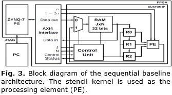
3.1.- BASELINE ARCHITECTURE
In this architecture (A1) the registers R0, R1, and R2 are connected in cascade to allow data streaming from memory. The term ujn+1 calculated by the stencil kernel is saved to the RAM via multiplexer. The block diagram is shown in Figure 3.
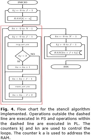
The flow chart for the stencil algorithm implemented is shown in Figure 4. Operations outside the dashed line are executed in PS and those found within the dashed line are executed in PL.
A performance counter is used to determine the number of clock cycles used to calculate all mesh points. This amount also can be calculated from the state machine sequence as shown in (4).
3.2.- HARDWARE LEVEL OPTIMIZATIONS
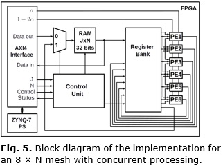
To increase the amount of space domain points that can be processed in one clock cycle more registers and PE are used. In Figure 5 is shown the implementation for an 8×N mesh, with six PE and a register bank for eight data. The control unit for this architecture (A2) has less states due to the J terms for the time step n+1 are obtained concurrently. To keep results available to calculate the values for the next time step without RAM access, the PE outputs are also stored at the same time in the register bank through internal multiplexers. With this configuration, the algorithm inner loop is simplified.
The concurrent processing improves the algorithm performance, but data storage is still sequential given that the system has only one RAM. Therefore, a memory structure that allows concurrent storage is proposed as shown in Figure 6. In this architecture (A3) the inner loop is suppressed from the control unit sequence.

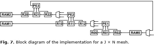
Although these architectures provide a better performance than the baseline architecture, the value of J is limited by the maximum number of PE allowed according to the FPGA physical resources. To achieve the treatment of problems involving larger mesh sizes in a single FPGA, the architecture shown in Figure 7 is proposed. This architecture uses the cascade registers as in the baseline architecture for the continuous reading of the data. In addition, a set of stencil cores and RAM blocks are used for data processing and storage. The arrangement of the registers, the PEs, and the RAMs, allows to perform the spatial and temporal sweep for handling of data dependencies.
4.- NUMERICAL RESULTS
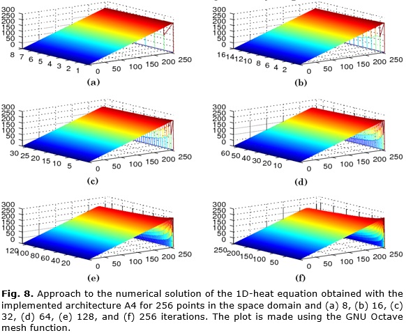
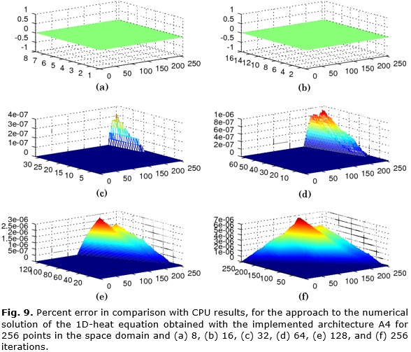
For initial values a ramp function is generated and send from PS section. Results of the approach to the numerical solution of the 1D-heat equation are stored in the SD card. Data values are printed in a text file using a precision format of 15 decimal digits. To visualize the results the mesh is plotted using GNU Octave. In Figure 8 is shown the meshes obtained with A4 for 256 points in the space domain and 8, 16, 32, 64, 128, and 256 iterations.
The percent error with respect to CPU results for the same mesh sizes, initial values, and boundary conditions is shown in Figure 9. Although the error obtained until iteration 256 does not exceed 7x10⁻⁶ %, it is observed that is accumulative with the increase of time steps.
5.- SYSTEM PERFORMANCE
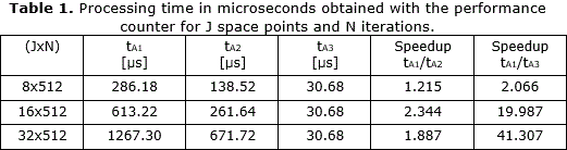
The processing time is measured using an internal counter enabled from control unit. The processing time in microseconds for 8, 16 and 32 points in the space domain and 512 iterations is shown in Table 1. The time for A3 does not vary with respect to number of PE given that it just depends on the number of iterations. The speed-up achieved with the parallel architectures (A2 and A3) is calculated in relation to the baseline architecture (A1).
To determine the system performance in terms of FLOPS, it is known that the stencil scheme implemented for the PE has four floating-point operations. Therefore, with a 100 MHz clock the system has a peak performance of 400 MFLOPS for A1 and 12 GFLOPS for A2 and A3. However, considering the number of mesh points, the stencil floating-point operations and the processing time, the performance achieved is shown in Table 2.

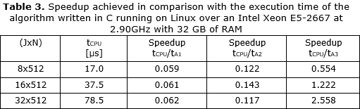
The speed-up achieved in comparison with the sequential algorithm written in C running on Linux over an Intel Xeon E5-2667 at 2.90GHz with 32 GB of RAM is shown in Table 3. The values of tCPU are the elapsed times used by the CPU processor to performs the nested loop.
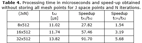
Performance can be improved for A2 if only the results of the iteration N are stored in the RAM. The processing time in microseconds and the speed-up achieved without storing all mesh for 512 iterations are shown in Table 4.
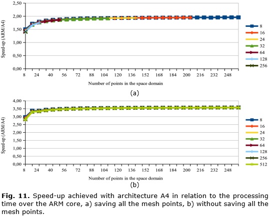
Although the architectures A2 and A3 improve the performance, they are limited in relation to the mesh size. On the other hand, the architectures A1 and A4 led to handle problems up to 256 points in the space domain and 512 iterations. In Figure 10 is shown the processing time in microseconds using A4, according to the number of iterations in function of the number of points in the space domain. It is observed that there is a proportional variation of the processing time both for the increase in the number of iterations and the number of points in the space domain.

From these results, the speed-up achieved in comparison with the sequential algorithm written in C running over the ARM core al 667 MHz is calculated. In Figure 11a is shown the speed-up when is used a bi-dimensional array and all the mesh points are stored in the RAM. The ARM has memory limitations when the algorithm is implemented using a bi-dimensional array, therefore the plot presents the comparisons for the allowed mesh sizes. In Figure 11b is shown the speed-up when is used a vector and only the terms of the last iteration are stored in the RAM.
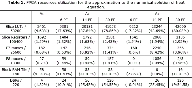
The FPGA resources utilization respect to the PE is summarized in Table 5 for A1, A2 and A3. This report corresponds to implementation using 65536x32 RAM for A1 and A2 and 512x32 RAM blocks for A3.
6.- CONCLUSIONS AND FUTURE WORK
In this paper is presented a system designed for the approach to the numerical solution of a parabolic PDE for a 1D heat transfer problem with initial value and boundary conditions using the explicit finite difference method. The implementation is made using the SoC architecture of a XC7Z020CLG484-1 Xilinx FPGA of the ZedBoard.
Four different architectures based in the stencil computation scheme are described. Performance analysis shows the improvement achieved in terms of the processing time for the stencil algorithm with the proposed architectures in relation to the embedded ARM processor. The speedup factor led to determine that implemented architectures offer different performance optimization due to the memory structure and control sequence. In all cases, the use of the registers array allows to take advantage of spatial and temporal locality reducing the need of memory transfer operations.
For future work, more deep performance analysis in terms of accuracy, precision, data transfer, scalability and power consumption could be performed. This evaluation should allow performance comparison with CPU and GPU based systems. Otherwise the design of variations for the implemented architectures to address 2D heat transfer problems using parabolic and elliptic PDEs could be developed. In addition, the obtained results could be compared with the software implementation of the stencil algorithm using high level synthesis tools.
ACKNOWLEDGEMENTS
This work was supported by the AE&CC research group of the Instituto Tecnológico Metropolitano through the project P14208. Luis Castaño acknowledges the financial support by the scholarship Estudiantes Sobresalientes de Posgrado Universidad Nacional de Colombia.
REFERENCES
1. Schmitt C, Schmid M, Hannig F, Teich J, Kuckuk S, Köstler H. Generation of Multigrid-based Numerical Solvers for FPGA Accelerators. 2nd International Workshop on High-Performance Stencil Computations. Amsterdam; The Netherlands. 2015 Jan: 9-15.
2. Usui T, Kobayashi R, Kise K. A Challenge of Portable and High-Speed FPGA Accelerator. In: Sano K, Soudris D, Hübner M, Diniz P. Applied Reconfigurable Computing: 11th International Symposium. Bochum(Germany): Springer International Publishing; 2015 Apr: 383-392.
3. Sano K, Hatsuda Y, Yamamoto S. Multi-FPGA Accelerator for Scalable Stencil Computation with Constant Memory-Bandwidth. IEEE Transactions on Parallel and Distributed Systems. 2014; 25(3): 695-705.
4. Kobayashi R, Kise K. Scalable stencil-computation accelerator by employing multiple FPGA. IPSJ Transactions on Advanced Computing Systems. 2013; 6(4): 1-13.
5. Bandishti V, Pananilath I, Bondhugula U. Tiling Stencil Computations to Maximize Parallelism. In: International Conference for High Performance Computing, Networking, Storage and Analysis. Salt Lake City(USA): IEEE Computer Society Press. 2012 Nov: 1-11.
6. Cecilia JM, Abellán JL, Fernández J, Acacio ME, García JM, Ujaldón M. Stencil computations on heterogeneous platforms for the Jacobi method: GPUs versus Cell BE. The Journal of Supercomputing. Springer US. 2012; 62(2): 787-803.
7. Kobayashi R, Takamaeda-Yamazaki S, Kise K. Towards a Low-Power Accelerator of Many FPGAs for Stencil Computations. International Conference on Networking and Computing. Naha(Japan): IEEE. 2012 Dec: 343-349.
8. Sano K, Hatsuda Y, Yamamoto S. Scalable Streaming-Array of Simple Soft-Processors for Stencil Computations with Constant Memory-Bandwidth. Annual International Symposium on Field-Programmable Custom Computing Machines. ç Salt Lake City (USA): IEEE. 2011 May: 234-241.
9. Strzodka R, Shaheen M, Pajak D, Seidel H. Cache Accurate Time Skewing in Iterative Stencil Computations. International Conference on Parallel Processing. IEEE. 2011 Sep: 571-581.
10. Brodtkorb AR, Dyken C, Hagen TR, Hjelmervik JM, Storaasli OO. State-of-the-art in heterogeneous computing. Scientific Programming. IOS Press. 2010; 18(1): 1-33.
11. Datta K, Kamil S, Williams S, Oliker L, Shalf J, Yelick K. Optimization and Performance Modeling of Stencil Computations on Modern Microprocessors. SIAM Review. 2009; 51(1): 129-159.
Received: December 15, 2016
Approved: April 10, 2017
Luis Castaño, Electronic Engineer, MEng Industrial Automation, PhD(c), Facultad de Ingeniería y Arquitectura, Universidad Nacional de Colombia, Manizales, Colombia. E-mail: lfcastanol@unal.edu.co. Professor, Facultad de Ingenierías, Instituto Tecnológico Metropolitano, Medellín, Colombia. E-mail: luiscastano@itm.edu.co.

